Contents
1. Introduction : Why Clearance and Creepage Matter in High-Voltage PCB Design
2. The Importance of Clearance and Creepage Distances in Preventing Electrical Failure
3. What Is Clearance Distance in PCB Design?
4. What Is Creepage Distance and Why It Matters in High-Voltage PCB Design
5. Clearance vs. Creepage Distance: What's the Difference and Why It Matters
6. Key Factors Affecting Clearance Distance
7. Key Factors Affecting Creepage Distance
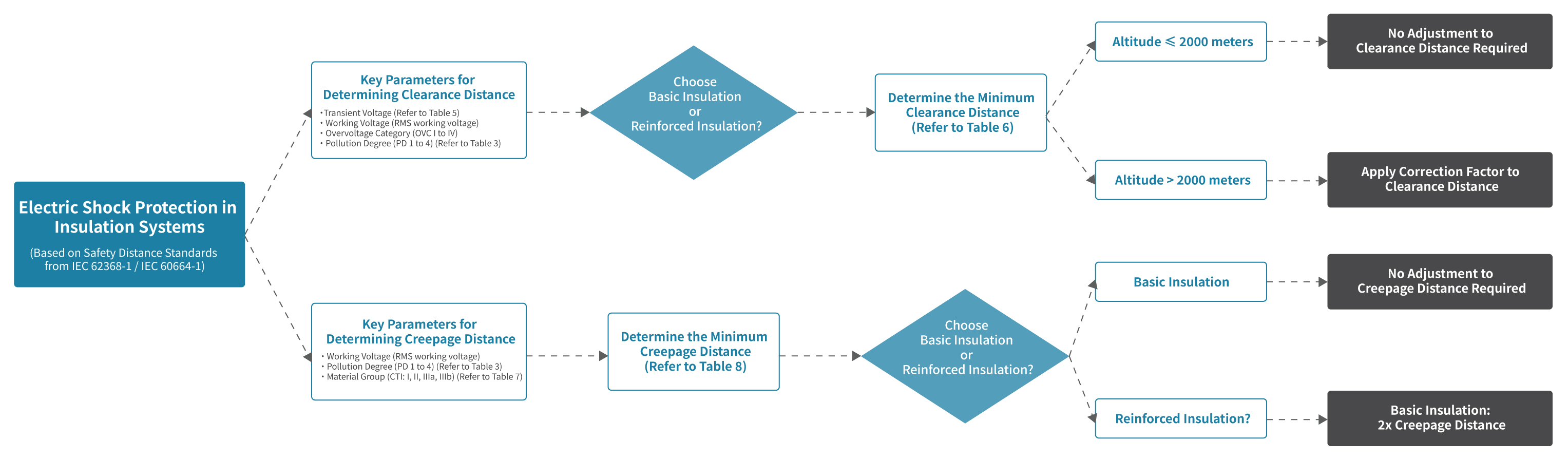
8. How to Determine Clearance and Creepage Distances (with Practical Example)
9. Frequently Asked Questions (FAQ) on Clearance and Creepage in PCB Design
10. Conclusion: Ensuring Safety with Proper Clearance and Creepage Design
Introduction : Why Clearance and Creepage Matter in High-Voltage PCB Design
As printed circuit boards (PCBs) continue to shrink in size while increasing in complexity and power density, every millimeter of board space has become critical. Pads, component leads, traces, and vias must be precisely laid out to ensure both space efficiency and electrical integrity.
In high-voltage applications—such as 800V power systems—the risks associated with inadequate spacing become much more severe. Insufficient insulation may lead to arcing, dielectric breakdown, or permanent component damage. Designers must also account for manufacturing needs, such as solder mask clearances, solder flow, and board separation during assembly.
That’s why clearance and creepage distances have become essential parameters in modern PCB design. They are critical for preventing failures caused by electrical stress, especially under conditions involving high voltages, humidity, or surface contamination. Understanding how to apply these concepts is fundamental to building safe, compliant, and reliable circuits that meet IEC and UL insulation standards.
The Importance of Clearance and Creepage Distances in Preventing Electrical Failure
Arcing typically occurs when the voltage between conductors exceeds the dielectric strength of the surrounding air, ionizing it and forming a conductive plasma path. This type of discharge can produce intense heat, visible light, and physical damage, often leading to system failure or even fire. These risks are especially pronounced in high-voltage circuits.
Another closely related hazard is dielectric breakdown. This happens when an insulating material is subjected to an electric field that exceeds its threshold, causing it to lose its insulating properties. The result? Current flows through unintended paths, accelerating material degradation and increasing the likelihood of short circuits.
To avoid such failures, clearance and creepage distances must be calculated based on the actual working voltage, pollution level, altitude, and insulation type. High-voltage or high-humidity environments often require larger spacing and more robust insulation strategies. By applying appropriate safety margins and adhering to standards such as IEC 60664-1 and IEC 62368-1 , designers can ensure long-term product reliability, user protection, and regulatory compliance.
What Is Clearance Distance in PCB Design?
Clearance distance is defined as the shortest path through air between two conductive elements at different electrical potentials. This spacing serves as a primary defense against high-voltage failures such as arcing and dielectric breakdown. When clearance is insufficient, the electric field strength may surpass the insulating capacity of air—causing ionization and forming a conductive path. This leads to an electrical arc, which can result in equipment damage, short circuits, or even fire.
In high-voltage PCB applications, ensuring proper clearance is crucial for maintaining insulation integrity. Factors like humidity, contamination, and installation altitude all influence air’s dielectric strength. For instance, higher humidity lowers breakdown voltage, making arcing more likely. Similarly, at altitudes above 2000 meters, thinner air provides less insulation.
To ensure long-term safety and compliance, PCB designers must calculate clearance distance in accordance with standards like IEC 60664-1 and IEC 62368-1, accounting for worst-case voltage, environmental conditions, and insulation requirements. Proper clearance not only prevents electrical failure but also extends product lifespan and operational stability.
.jpg)
Figure 1. Illustration of Clearance Distance between Conductive Parts
What Is Creepage Distance and Why It Matters in High-Voltage PCB Design
Creepage distance is defined as the shortest path along the surface of an insulating material between two conductive parts at different electrical potentials. Unlike clearance, which goes through air, creepage follows the contours of the insulating surface—making it especially vulnerable to contamination, dust, moisture, or debris. These surface contaminants can create conductive paths that lead to insulation breakdown, leakage currents, and even short circuits.
Poor surface conditions or low-quality insulation materials can reduce dielectric strength and compromise long-term reliability. For this reason, determining the proper creepage distance is crucial for high-voltage and safety-critical PCB applications. The required creepage depends on working voltage, pollution degree, surface tracking characteristics, and the Comparative Tracking Index (CTI) of the insulation material.
Designers should refer to international standards such as IEC 60664-1 when calculating creepage requirements. By selecting the right materials and designing sufficient spacing, you reduce the risk of failure, enhance product durability, and ensure compliance with safety regulations in demanding environments.
.jpg)
Clearance vs. Creepage Distance: What's the Difference and Why It Matters
Clearance and creepage are two essential insulation parameters in PCB and high-voltage system design. While they both aim to prevent electrical failures, each addresses different electrical risks and requires unique layout considerations.
| Attribute | Clearance | Creepage |
|---|---|---|
| Medium | Shortest distance through air | Shortest distance along the surface of insulation |
| Main influencing factors | Voltage, altitude, air humidity, temperature | Pollution degree, humidity, CTI, surface condition |
| Primary purpose | Prevent arcing and electrical breakdown | Prevent surface tracking and leakage currents |
Key Factors Affecting Clearance Distance
To determine appropriate clearance distance in high-voltage PCB designs, international standards such as IEC 62368-1 and IEC 60664-1 recommend evaluating the following key parameters:
- .Working Voltage: This is the maximum voltage expected under normal operating conditions. Higher working voltages require larger clearance to avoid air dielectric breakdown and arcing.
- .Overvoltage Category (OVC): Defines the expected level of transient overvoltages based on the installation environment. Higher OVC levels demand greater insulation strength and spacing.
- .Pollution Degree: Reflects the level of environmental contamination (e.g., dust, moisture). A higher pollution degree increases the likelihood of breakdown and requires larger clearance.
- .Type of Insulation: Different insulation levels—such as basic, supplementary, double, or reinforced insulation—each have unique clearance requirements.
- .Installation Altitude: Higher altitudes reduce air density and its dielectric strength. As elevation increases, clearance distance must be corrected using altitude factors.
- .Transient Overvoltage: Short-duration voltage spikes must be factored in, as they can exceed the normal working voltage and compromise insulation.
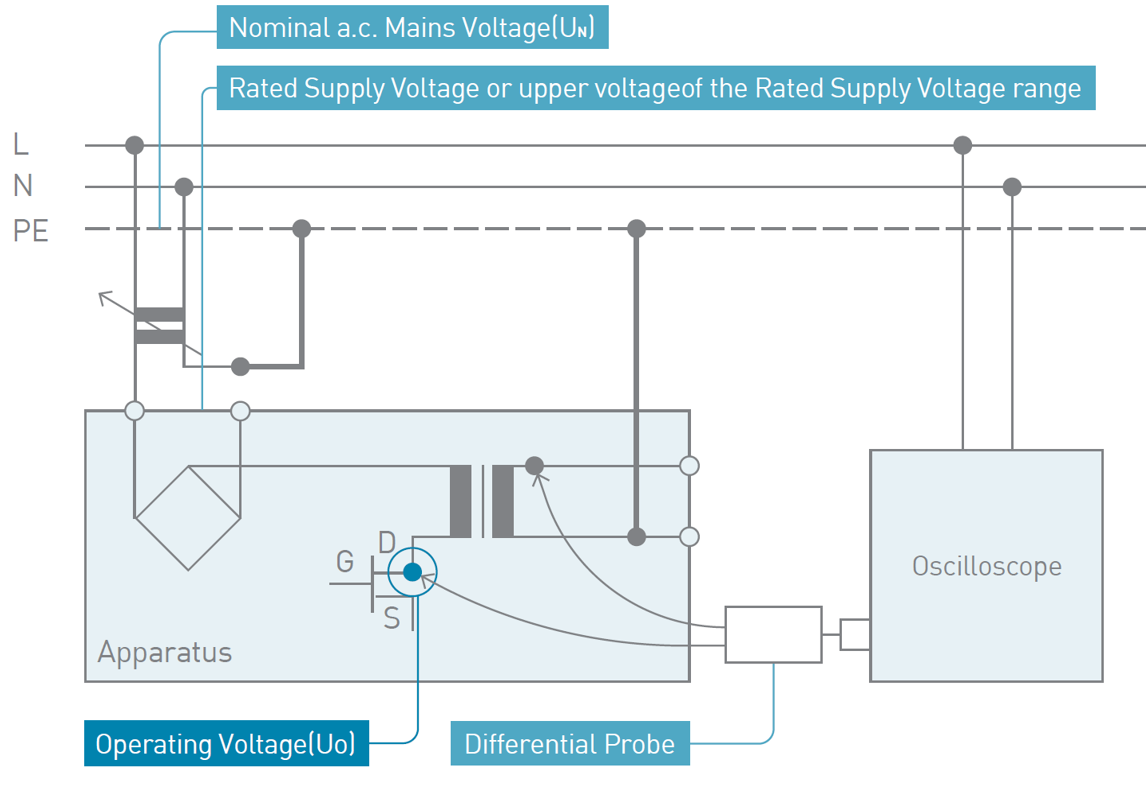
1、Working Voltage
In insulation design, working voltage refers to the continuous voltage applied across the insulation barrier during normal operation. It directly impacts the required clearance and creepage distances in PCB layouts. According to IEC 62368-1, working voltage is defined as the maximum RMS or DC voltage between secondary circuits under normal conditions.
- .Peak Value: The highest instantaneous voltage within a waveform cycle.
- .RMS Value: The root-mean-square value used to assess heating effect and insulation requirements over time.
2、Overvoltage Category (OVC)
Overvoltage Category classifies the level of transient overvoltage risk that equipment might encounter. It directly influences the minimum required clearance distance. IEC 62368-1 defines four categories:
Higher category = Higher insulation demand.
| Overvoltage category | Equipment and its point of connection to the a.c. mains | Examples of equipment |
|---|---|---|
| IV | Equipment that will be connected to the point where the mains supply enters the building |
- Electricity meters - Communications ITE for remote electricity metering |
| III | Equipment that will be an integral part of the building wiring |
- Socket outlets, fuse panels and switch panels - Power monitoring equipment |
| II | Pluggable or permanently connected equipment that will be supplied from the building wiring |
- Household appliances, portable tools, home electronics - Most ITE used in the building |
| I | Equipment that will be connected to a special mains in which measures have been taken to reduce transients | - ITE supplied via an external filter or a motor driven generator |
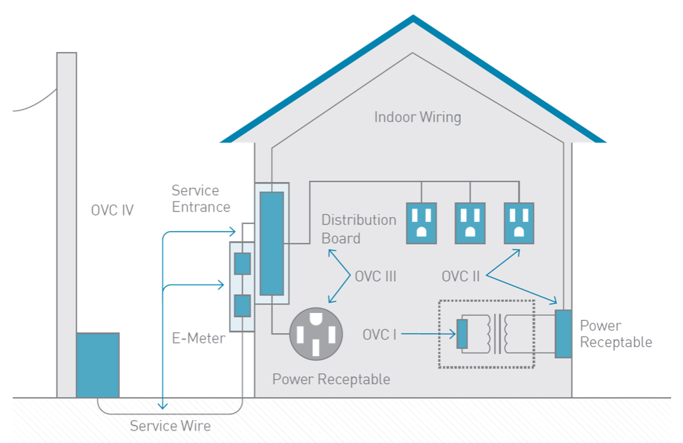
Figure 4. Reference Locations of Equipment Connection to AC Mains by Overvoltage Category
3、Pollution Degree
Pollution degree classifies the environment's potential to cause conductive contamination. It affects both clearance and creepage requirements.
| Classes | Descriptions | Examples |
|---|---|---|
| Pollution degree 1 | There is no pollution or only dry, nonconductive pollution | Sealed components (coated PCB), clean room |
| Pollution degree 2 | Temporarily becomes conductive because of occasional condensation |
|
| Pollution degree 3 |
|
Industrial, unheated factory rooms and farming |
| Pollution degree 4 | Continuous conductivity occurs because of conductive dust, rain or other wet conditions | Outdoor applications |
4、Type of Insulation
The insulation class determines how much protection is required against electric shock and system failure. Each type demands different spacing and material specifications:
- .Functional Insulation: Needed for operation only; no user protection.
- .Basic Insulation: One layer of protection; not sufficient alone.
- .Supplementary Insulation: Extra layer that backs up basic insulation.
- .Double Insulation: Basic + supplementary = enhanced safety.
- .Reinforced Insulation: Single layer equivalent to double insulation; must meet minimum thickness (e.g., 0.4 mm per IEC 62368-1).
5、Installation Altitude
At altitudes above 2000 meters, reduced air pressure leads to lower dielectric strength, requiring increased clearance.
Apply correction factors from IEC 62368-1 to maintain compliance.
| Altitude (m) |
Normal barometric pressure (kPa) |
Multiplication factor for clearances |
Multiplication factor for electric strength test voltages | |||
|---|---|---|---|---|---|---|
| ≥0,01 mm to | ≥0,0625 mm to | ≥1 mm to | ≥10 mm to | |||
| 2000 | 80,0 | 1,00 | 1,00 | 1,00 | 1,00 | 1,00 |
| 3000 | 70,0 | 1,14 | 1,05 | 1,05 | 1,07 | 1,10 |
| 4000 | 62,0 | 1,29 | 1,10 | 1,10 | 1,15 | 1,20 |
| 5000 | 54,0 | 1,48 | 1,17 | 1,16 | 1,24 | 1,33 |
6、Transient Voltage
Transient overvoltages (e.g., from lightning or switching) can exceed working voltage and lead to breakdown. Required clearance distances must align with transient voltage levels defined per OVC and AC mains voltage.
| AC Mains Voltage |
Transient Voltage V peak |
||||
|---|---|---|---|---|---|
|
RMS Voltage (V r.m.s.) |
Peak Voltage (V peak) |
I | II | III | IV |
| 50 | 71 | 330 | 500 | 800 | 1500 |
| 100 | 141 | 500 | 800 | 1500 | 2500 |
| 150 | 210 | 800 | 1500 | 2500 | 4000 |
| 300 | 420 | 1500 | 2500 | 4000 | 6000 |
| 600 | 840 | 2500 | 4000 | 6000 | 8000 |
|
Required withstand voltage V peak or d.c. |
Basic insulation or supplementary insulation (mm) |
Reinforced insulation (mm) |
||||
|---|---|---|---|---|---|---|
| Pollution degree 1⁽ᵃ⁾ | Pollution degree 2 | Pollution degree 3 | Pollution degree 1⁽ᵃ⁾ | Pollution degree 2 | Pollution degree 3 | |
| 330 | 0.01 | 0,2 | 0,8 | 0.02 | 0,4 | 1,5 |
| 400 | 0,02 | 0,04 | ||||
| 500 | 0,04 | 0,08 | ||||
| 600 | 0,06 | 0,12 | ||||
| 800 | 0,10 | 0,20 | ||||
| 1000 | 0,15 | 0,30 | ||||
| 1200 | 0,25 | 0,5 | ||||
| 1500 | 0,50 | 1,0 | ||||
| 2000 | 1,00 | 2,0 | ||||
| 2500 | 1,50 | 3,0 | ||||
| 3000 | 2,00 | 3,8 | ||||
| 4000 | 3,00 | 5,5 | ||||
| 5000 | 4,00 | 8,0 | ||||
Table 6. Minimum Clearance Distances Corresponding to Required Withstand Voltages
Key Factors Affecting Creepage Distance
To ensure safety in high-voltage PCB design, the required creepage distance must be determined in accordance with international standards such as IEC 60664-1. The following five factors play a critical role in defining minimum creepage spacing between conductive elements:
- .Working Voltage: The rated working voltage during normal operation directly determines the minimum required creepage. Higher voltages increase the risk of surface breakdown, necessitating greater insulation distance.
- .Pollution Degree: A higher pollution degree indicates a more contaminated environment (e.g., dust, humidity), which increases the likelihood of conductive paths forming on insulating surfaces. Consequently, this requires longer creepage distances to maintain electrical safety.
- .Type of Insulation: The insulation category—whether basic, supplementary, double, or reinforced insulation—dictates the creepage distance. Higher insulation classes generally require more separation to meet safety requirements.
- .CTI (Comparative Tracking Index): The CTI value of a material measures its resistance to surface tracking. Materials with higher CTI ratings allow for shorter creepage distances, as they are more resistant to degradation under electrical stress.
- .Type of Voltage: The waveform type—AC, DC, or impulse voltage—also affects surface degradation behavior. Impulse voltages can accelerate insulation wear, requiring adjustment in creepage design.
Comparative Tracking Index(CTI)
The Comparative Tracking Index (CTI) is a key material property used in determining minimum creepage distance. It measures an insulating material’s ability to withstand electrical surface tracking, which can result in progressive degradation and potential failure of the insulation layer.
A higher CTI value means the material is more resistant to electrical tracking, and thus permits shorter creepage distances. This is particularly important in high-voltage or high-contamination environments.
Under IEC 60664-1, insulating materials are categorized into four groups based on their CTI values:
| Material groups | CTI range (VRMS) |
|---|---|
| Material group I | CTI ≥ 600 |
| Material group II | 400 ≤ CTI |
| Material group IIIa | 175 ≤ CTI |
| Material group IIIb | 100 ≤ CTI |
- .CTI value of the material (plastic or PCB)
- .Pollution Degree of the environment
- .Rated Working Voltage of the circuit
|
RMS working voltage up to and including V |
1⁽ᵃ⁾ |
Pollution degree 2 Material group |
Pollution degree 3 Material group |
||||
|---|---|---|---|---|---|---|---|
| I, II, IIIa, IIIb | II | IIIa, IIIb | I | II | IIIa, IIIb see Note |
||
| 10 | 0,08 | 0,4 | 0,4 | 0,4 | 1,0 | 1,0 | 1,0 |
| 12,5 | 0,09 | 0,42 | 0,42 | 0,42 | 1,05 | 1,05 | 1,05 |
| 16 | 0,1 | 0,45 | 0,45 | 0,45 | 1,1 | 1,1 | 1,1 |
| 20 | 0,11 | 0,48 | 0,48 | 0,48 | 1,2 | 1,2 | 1,2 |
| 25 | 0,125 | 0,5 | 0,5 | 0,5 | 1,25 | 1,25 | 1,25 |
| 32 | 0,14 | 0,53 | 0,53 | 0,53 | 1,3 | 1,3 | 1,3 |
| 40 | 0,16 | 0,56 | 0,8 | 1,1 | 1,4 | 1,6 | 1,8 |
| 50 | 0,18 | 0,6 | 0,85 | 1,2 | 1,5 | 1,7 | 1,9 |
| 63 | 0,2 | 0,63 | 0,9 | 1,25 | 1,6 | 1,8 | 2,0 |
| 80 | 0,22 | 0,67 | 0,95 | 1,3 | 1,7 | 1,9 | 2,1 |
| 100 | 0,25 | 0,71 | 1,05 | 1,4 | 1,8 | 2,0 | 2,2 |
| 125 | 0,28 | 0,75 | 1,15 | 1,5 | 2,0 | 2,2 | 2,4 |
| 160 | 0,32 | 0,8 | 1,25 | 1,6 | 2,1 | 2,3 | 2,5 |
| 200 | 0,42 | 1,0 | 1,4 | 2,0 | 2,5 | 2,8 | 3,2 |
| 250 | 0,56 | 1,25 | 1,8 | 2,5 | 3,2 | 3,6 | 4,0 |
| 320 | 0,75 | 1,6 | 2,2 | 3,2 | 4,0 | 4,5 | 5,0 |
| 400 | 1,0 | 2,0 | 2,8 | 4,0 | 5,0 | 5,6 | 6,3 |
| 500 | 1,3 | 2,5 | 3,6 | 5,0 | 6,3 | 7,1 | 8,0 |
| 630 | 1,8 | 3,2 | 4,5 | 6,3 | 8,0 | 9,0 | 10 |
| 800 | 2,4 | 4,0 | 5,6 | 8,0 | 10 | 11 | 12,5 |
| 1000 | 3,2 | 5,0 | 7,1 | 10 | 12,5 | 14 | 16 |
| 1250 | 4,2 | 6,3 | 9,0 | 12,5 | 16 | 18 | 20 |
| 1600 | 5,6 | 8,0 | 11 | 16 | 20 | 22 | 25 |
| 2000 | 7,5 | 10 | 14 | 20 | 25 | 28 | 32 |
| 2500 | 10 | 12,5 | 18 | 25 | 32 | 36 | 40 |
Table 8. Minimum Creepage Distances for Basic Insulation
How to Determine Clearance and Creepage Distances (with Practical Example)
When designing high-voltage electronic systems , calculating clearance and creepage distances is a critical part of PCB safety planning. To illustrate the process, here’s a step-by-step insulation distance calculation using a real-world example from MINMAX’s AMF-07 Series AC-DC converter.
※This calculation method aligns with the general MINMAX product design process and is intended for engineering reference.
Insulation Distance Calculation Example
Let’s take the MINMAX AMF-07 Series AC-DC power supply as an example:
Assumed Parameters
- .Input AC Range: 85–264VAC (Maximum working voltage: 250Vrms)
- .Overvoltage Category: OVC II
- .Pollution Degree: PD2
- .Installation Altitude: 5,000 meters
- .CTI Group: IIIa, IIIb
A. Clearance Distance Calculation
1. Based on Table 5, for a maximum working voltage of 300V and OVC II, the required transient withstand voltage is 2500V peak.
2. Referencing Table 6, the required clearance distance under basic insulation is 1.5 mm, and under reinforced insulation, it is 3.0 mm.
3. At 5000 meters altitude, a correction factor must be applied. According to Table 4, the adjusted clearance becomes:
• Basic insulation → 1.5 mm × 1.48 = 2.22 mm
• Reinforced insulation → 3.0 mm × 1.48 = 4.5 mm
B. Creepage Distance Calculation
1. From Table 8, using 250Vrms, cross-referencing PD2 and CTI group IIIa/IIIb, the minimum creepage distance under basic insulation is 2.5 mm.
2. For reinforced insulation, the required creepage is 2× basic insulation, which is 5.0 mm (2.5 mm × 2).
Note: Creepage distance is not affected by altitude. It is determined solely by the CTI rating, pollution degree, and working voltage.
Frequently Asked Questions (FAQ) on Clearance and Creepage in PCB Design
1. What is the difference between clearance and creepage distance?
Clearance is the shortest distance through air between two conductive parts, while creepage is the shortest distance along the surface of an insulating material. Both are critical to prevent arcing and surface leakage.
2. Why are clearance and creepage distances important in high-voltage PCB design?
They prevent insulation failure caused by electrical arcing or surface tracking. Inadequate spacing can lead to dielectric breakdown, short circuits, or safety hazards, especially in high-voltage systems.
3. How does pollution degree affect creepage distance?
A higher pollution degree indicates more contaminants on the surface, increasing the risk of leakage currents. This requires a longer creepage distance to maintain insulation reliability.
4. Do clearance and creepage requirements change with altitude?
Yes. Clearance distances must be increased at high altitudes due to reduced air dielectric strength. Creepage distances are not affected by altitude but depend on surface conditions and CTI values.
5. What is the role of CTI in determining creepage distance?
CTI (Comparative Tracking Index) measures a material’s resistance to surface tracking. A higher CTI allows for shorter creepage distances under the same pollution degree and voltage level.
6. Which standard should I follow—IEC 60664-1 or IEC 62368-1?
IEC 60664-1 provides the basis for insulation coordination and distance calculation, while IEC 62368-1 applies to the safety of audio/video, IT, and communication equipment. Use both in tandem, depending on product type.
Conclusion: Ensuring Safety with Proper Clearance and Creepage Design
Accurately defining clearance and creepage distances is vital to maintaining the safety, performance, and regulatory compliance of electronic equipment—especially in high-voltage, polluted, or high-altitude environments. These physical insulation distances help prevent electrical arcing, leakage currents, and dielectric breakdown, which can lead to system failure or safety hazards.
By understanding and applying standards like IEC 60664-1 and UL, engineers can build robust PCB layouts and power systems that withstand harsh operating conditions and meet global safety requirements.
At MINMAX Technology, all of our isolated DC-DC and AC-DC converters are engineered with these insulation factors in mind. Our products are tested to meet stringent international certifications such as IEC 62368-1, UL 62368-1, and EN standards. These converters are ideal for use in industrial control systems, medical electronics, and telecom equipment—where insulation safety is mission-critical.
📞 Contact MINMAX for Expert Support
Need help with insulation distance design or power module selection?
👉 Get in touch with the MINMAX technical team for personalized advice and compliance-ready solutions.
For more Technical Articles>>>
To learn more, please click on the following link:
【MINMAX Industrial Power Solution】
【MINMAX Railway Power Solution】
【MINMAX High Isolation and Voltage Resistant Power Supply Solution】